RACOMTECH is a professional RF & Microwave technology company, our RF & Microwave...
Read moreCatalog
- –Test Instruments
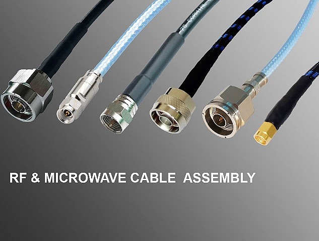
- –Coaxial Cable & Assemblies
- –RF Components
- –RF Connectors
- –Coax Adapters
- –2.92mm
- –3.5mm
- –4.3/10 to N, 716
- –BNC - UHF
- –F to BNC
- –In series BNC
- –In series DIN 716
- –In series N type
- –In series RP-SMA
- –In series SMA
- –In series TNC
- –In series UHF
- –N Type - BNC
- –N Type - DIN716
- –N type - F adapter
- –N type - MCX
- –N type - RP-SMA /
- –N Type - SMA
- –N type - SMB
- –N Type - TNC
- –N Type - UHF
- –RP-SMA / RP-TNC
- –SMA - F adapter
- –SMA - RP-SMA
- –SMA / BNC Adapter
- –SMA / TNC adapters
- –SMA / UHF adapters
- –TNC / RP-SMA / BNC
- –K 2.92mm
- –3.5mm
- –N type
- –SMA
- –TNC
- –7/16 DIN
- –4310
- –BNC
- –FME
- – F
- –MCX
- –SMB
- –UHF
- –Coax Adapters
- –Tools & Soldering Station
- –Custom Design
- –Clearance Centre
Information
LatestCable Catalogue
Ournews
-
01/28/2020
-
04/01/2018
The VSWR ( The voltage standing wave ratio ) is a measure of impedance match of load to the transmission line....
Read more -
03/31/2018
The outer conductor size of these connectors prevents the mating of incompatible connectors....
Read more -
03/21/2018
Simplified EMI PreCompliance & Debug RSA5000 SERIES SPECTRUM ANALYZERS High Performance Real-Time Spectrum...
Read more
Monolithic Amplifier VNA 25 ( 0.5-2.5 GHz / 18.2dBm )
")
")
")
Category:
Components for sale
Description
Reviews (0)
Features
Overview
Product Features
3V & 5V operation
no external biasing circuit required
internal DC blocking at RF input and output
Gain, 17 dB typ.
wide bandwidth, 0.5 to 2.5 GHz
low noise figure, 5.5 dB typ.
output power, up to +18.2 dBm typ.
low cost
Typical Applications
buffer amplifier (LO Amplifier)
cellular, Lband, WiFi Amplifier
PCN
Pin Description
Function Pin number Description
RF IN 3 RF input pin.
RF OUT 6 RF output pin.
DC 1 Bias pin
GND 2,4,5,7,8
Connections to ground. Use via holes as shown in Suggested Layout for PCB
Design to reduce ground path inductance for best performance.
General Description
VNA-25 is a wideband amplifi er offering high dynamic range. It has repeatable performance from lot to
lot. It is enclosed in an 8-lead SOIC package. VNA-25+ is fabricated using GaAs MESFET technology.
Expected MTBF at 85°C case temperature is 40,000 years at 2.8V, 2,000 at 5V.
VNA25 Datasheet_1 ![]() Data sheet Minicircuits
Data sheet Minicircuits![]()
Manufacture: Minicircuits
Features
| WEIGHT (Packed) | 0.02 kg |
| Qty. Order | 1, 10 ((Save 10%), 50 (Save 20%) |